


Revolutionized is reader-supported. When you buy through links on our site, we may earn an affiliate commision. Learn more here.
3D printers have proven to be a truly consequential innovation. Hobbyists and companies everywhere are regularly discovering new applications for these devices. One of the latest involves 3D-printed electronic circuits.
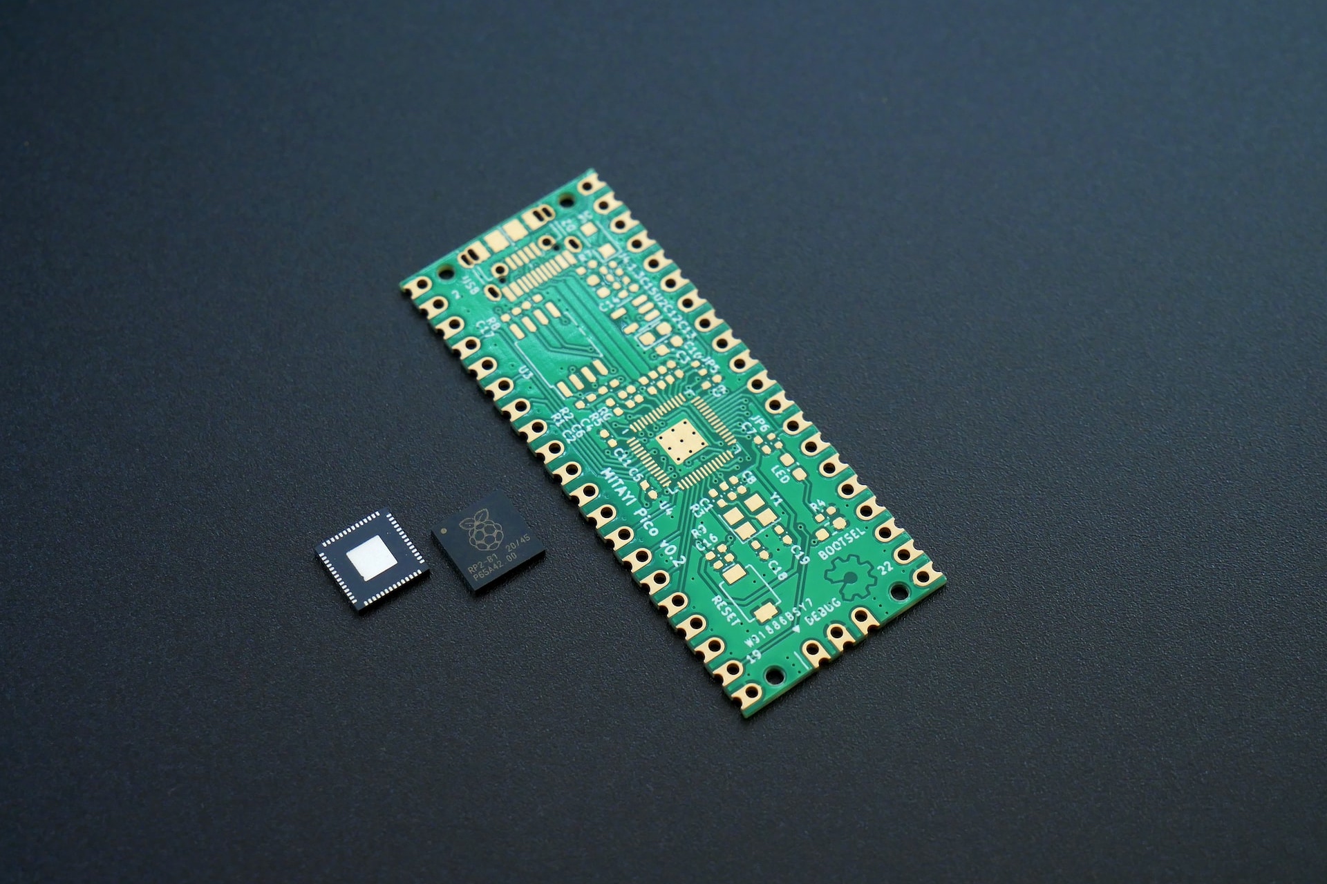
Printed circuit boards (PCBs) are some of the most important components within modern electronic devices. They provide electrical and mechanical features that allow elements in the device – like semiconductors, capacitors, wireless radios, and more – to communicate with one another.
From smartphones to garage door openers, PCBs are everywhere – and they’re vital for modern living. 3D printers may give us new ways to shore up production of these components at a time when sourcing them can be difficult. What are 3D-printed electronic circuits? Do they have limitations compared to conventional electronic circuit boards? It turns out they may be just as capable as their conventional counterparts, and perhaps more so.
There are two primary methods that machine operators can use when it comes to 3D printing electronic circuits: Conductive filaments or hollow trenches. Here’s a breakdown of the differences:
No matter which method you’re interested in, perhaps the more important question is: What advantages do 3D printers demonstrate over their more conventional counterparts?
The first method – 3D printing the chosen circuitry pattern onto the PCB using conductive materials – unlocks new design possibilities. Although not widely explored at scale yet, this method could allow designers to create circuits and circuit boards in brand-new shapes and form factors. It could also allow multiple circuitry layers at once.
But what about comparing the two 3D printing methods directly?
Using conductive filament has the advantage of greater accuracy and the potential to create more complicated shapes than the trench method.
However, creating hollow trenches using a 3D printer is a more straightforward process that requires less finesse and expertise. It also doesn’t require solder. But the end cost may be higher because it requires sourcing conductive filler.
Both methods introduce greater flexibility to the printed circuit board design and fabrication process. 3D printers as a manufacturing asset are more adaptable. They also allow for quicker tool changeovers and design revisions as project needs dictate.
People must not overlook the previously mentioned advantage involving multi-layered circuitry designs and new form factors. 3D printing helps technologists and engineers to deliver more capable, personalized, physiology-friendly an space-efficient technology. This ranges from implantable health devices, like pacemakers, to smart watches, cell phones, laptops, networking equipment, internet of things (IoT) networks, and classes of products we haven’t even envisioned yet.
Designers have previously faced the limitations of conventional manufacturing methods, like injection molding and CNC machining. Both of these disciplines still have a place in modern manufacturing, including some projects involving electronic circuits, but 3D printing may be earning its place as the primary fabrication method in this field and others.
3D-printed electronic circuits are an impressive development that will only continue to receive refinement. As they do, we should see an explosion of innovation and design novelties in the various electronic device markets.
Revolutionized is reader-supported. When you buy through links on our site, we may earn an affiliate commision. Learn more here.


This site uses Akismet to reduce spam. Learn how your comment data is processed.